Teardown / Assembly of a 90s PC
20 Nov 2020 | 20 minutes to readI received many of the parts for this computer when an acquaintance was moving out of their old house. It looked like it hadn’t worked in several years, and sadly wasn’t able to for this article (faulty PSU). Regardless, I wanted to stuff it full of parts and catalog everything in an obituary of sorts, though I hope to eventually get it working. I see this computer as an interesting time capsule of what a late 90’s computer would be equipped with.
This computer is very interesting because it bridges the divide between new and old system technologies present during the 90s. It has a wide range of expansions slots and even the ability to use two different types of power supplies. Let’s get into it!
The Case
The case is a small, normal looking beige case. It looks like any other case of the period. The case dimensions are H 13” x L 16” x W 7”, and has space inside for an micro ATX motherboard.
Front Panel
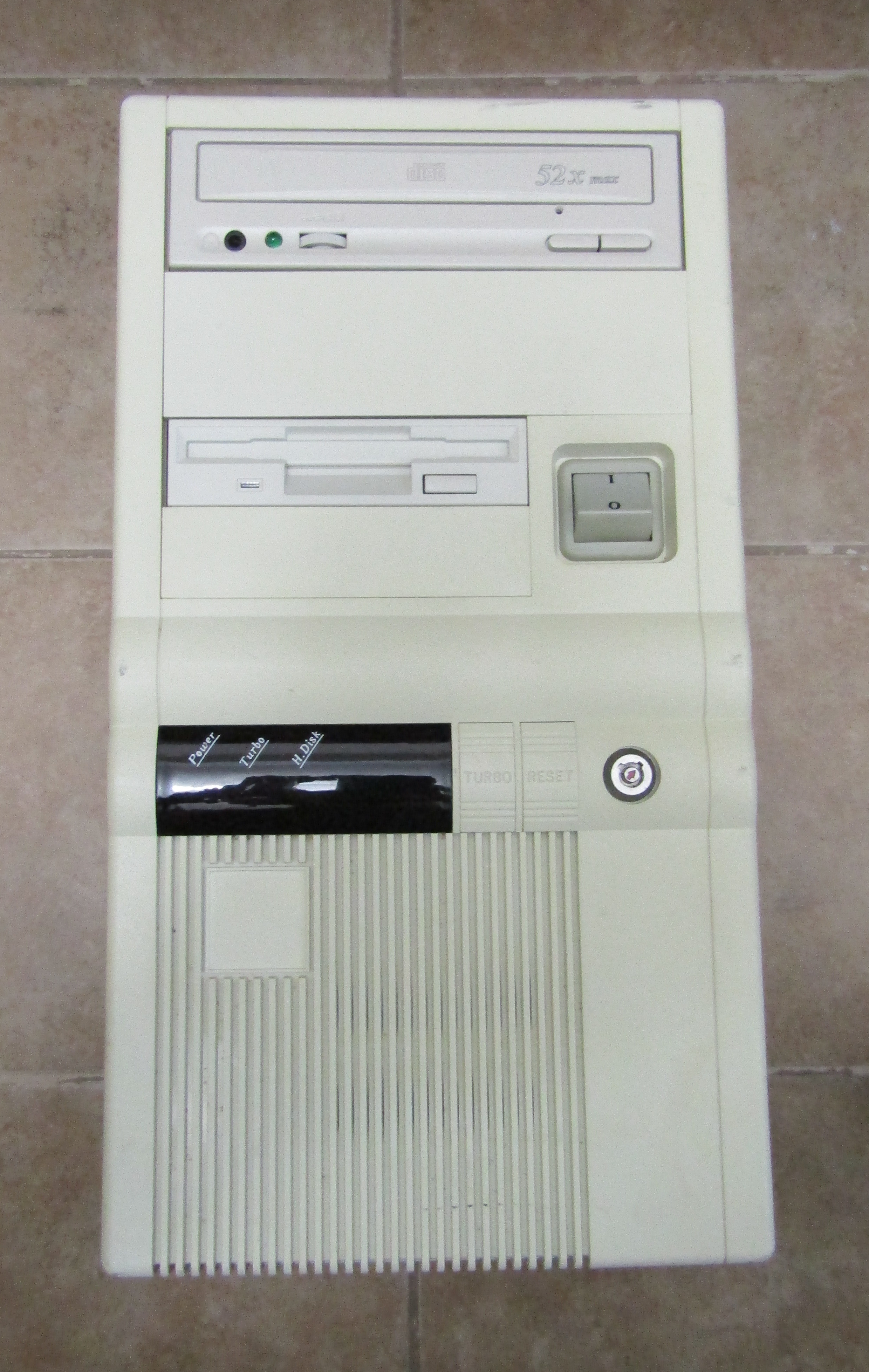
The front of the case it outfitted with your normal fare of slots and buttons. At the top there is two slots for disk drives and two slots for floppy drives. To the left of the floppy disk drive slots is the On/Off toggle switch. It gives a satisfying “thunk” when switching it.
Below that is the array of activity LED’s, more buttons, and the case lock. It gives you power, turbo, and hard disk activity LEDs behind some transparent dark plastic. It looks as though the case would also support a 7-segment display to show clock speed, but this model didn’t come with it installed. Instead, there is an empty square hole between the activity LEDs.
The turbo and reset buttons are placed beside the plastic LED cover. The turbo button is a toggle switch like the power button, and the reset a simple push-button switch. Besides those is the case lock, which allows the user to lock/unlock the motherboard. When locked, it wouldn’t allow the computer to start.
Finally, underneath the lights is an empty space for the computer badge. It currently is empty, but I would eventually like to put something there, either a AMD processor badge or a badge for whatever OS ends up running on the computer (OS/2?).
Back Panel
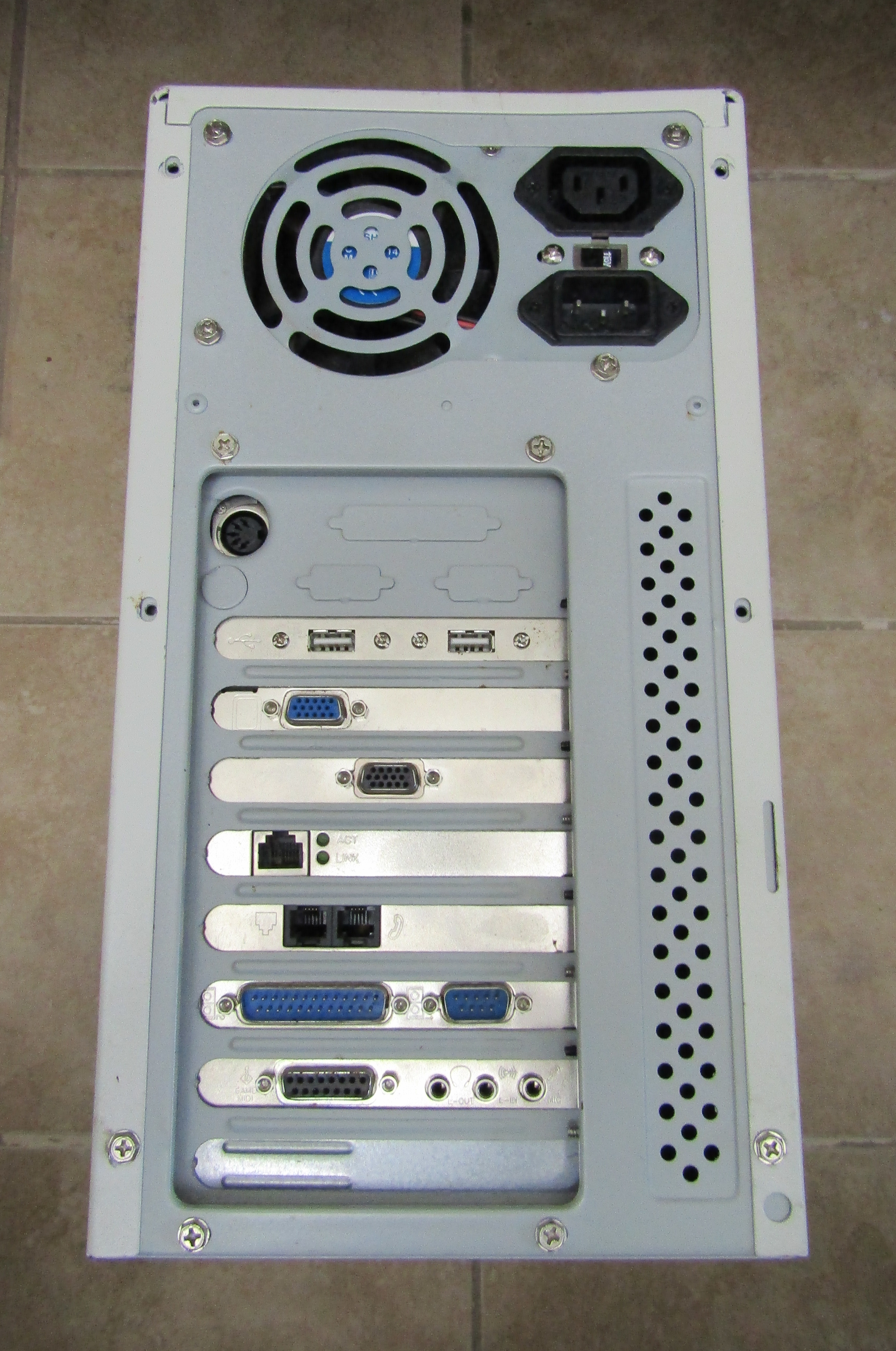
The power supply is mounted at the top of the case. Visible is the fan opening, two cable ports and a small switch to toggle between 115V and 230V. The two separate power cable ports support the C13 (Common female type) and C14 (Uncommon male type) ends.
There are 8 expansion slot spots for various cards to be mounted. I’ve got 7 of them filled with a variety of cards, and the last has a metal cover over it. Right above the slots is a column of air holes, the only place on the back for air to be exchanged with the main cavity of the case.
It does not have a mounting spot for an I/O plate, instead opting to have only a few panel mounting spots for ports. There are two peripheral holes, one for the AT Keyboard port and one for a PS/2 port. The case is setup specifically for the motherboard inside, so only the AT port is open. The PS/2 port still has some case metal over it. There are also a few covered serial cable mount spots, two for 9-pin serial connectors, and one for a 25-pin connector.
Inside the Case
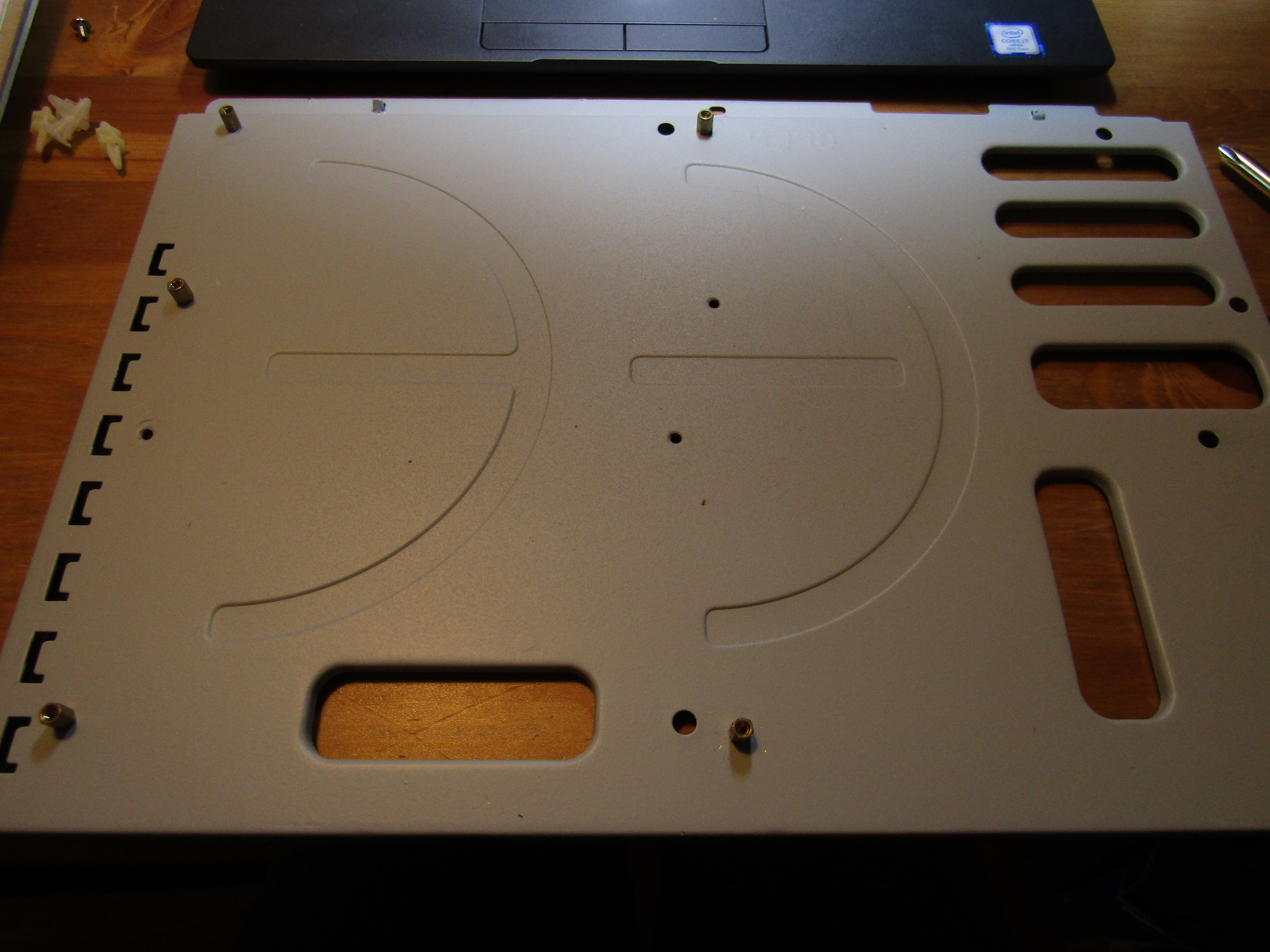
This case is interesting, in that it has a separate tray on which to attach the motherboard. Once everything is unplugged, it makes it pretty easy to pull out the motherboard and swap out parts without needing to work around the case itself. Originally, it had cheap plastic standoffs that separated the motherboard from the metal tray but they had become chipped and broken so I opted to replace them with nicer metal ones that allow screws to be used.
The power supply for the system seemed to come with the case, as there is a dedicated cord from the power supply to the toggle switch on the front. Unlike normal “On” buttons which are simple push button switches, this one is a toggle switch. I love it, as it gives a nice satisfying clunk when switched to on or off.
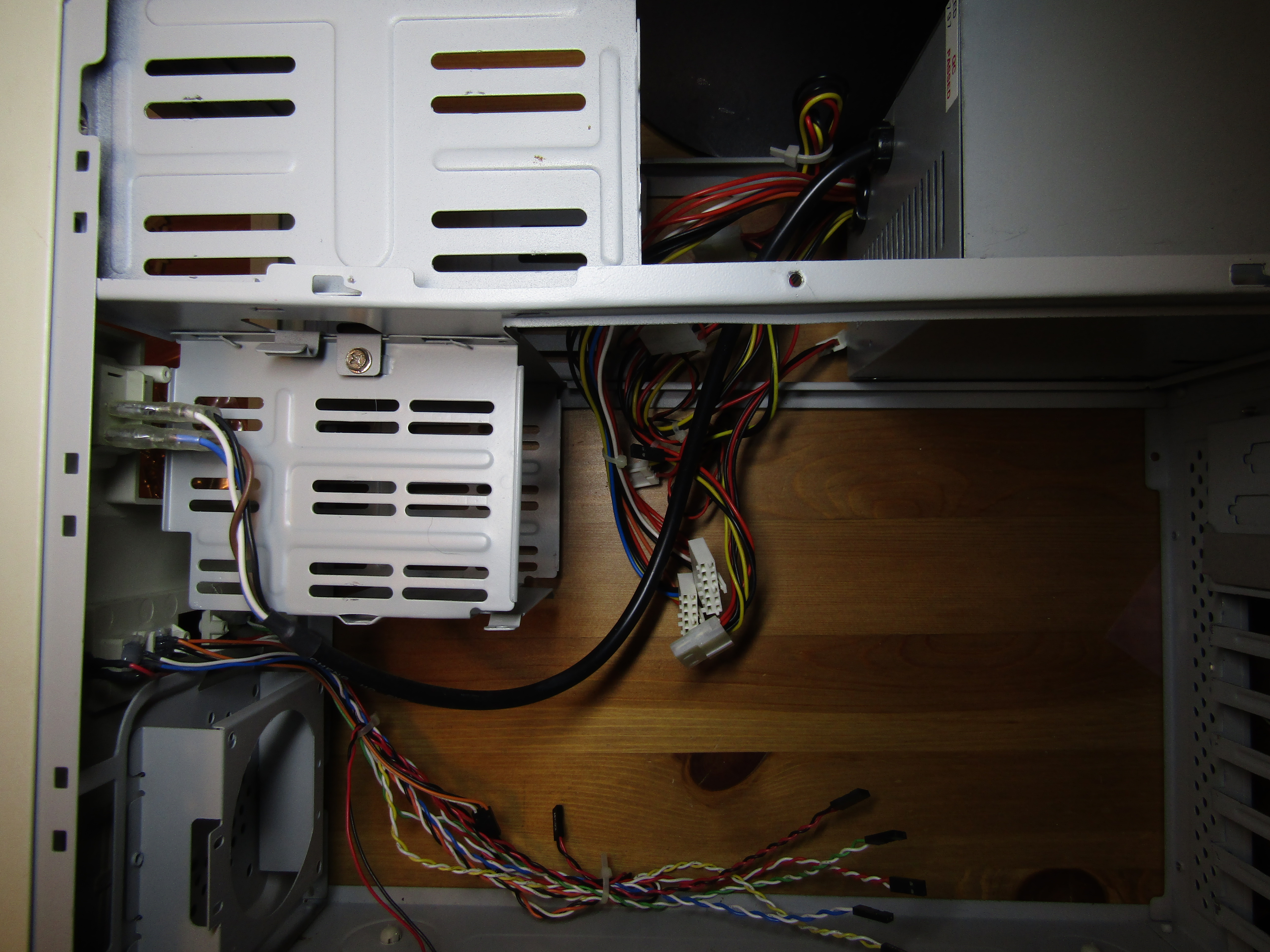
The built in case speaker mounts and projects out the bottom. It would have been only useful for making beeping noises, which is why a sound card was also installed on the computer. The only fan exhaust seems to be in the front. While there is a grille in the back, the front has a spot where a use could mount a small fan. It wouldn’t be too effective though, the cutouts for air on the front of the case wouldn’t have allowed much air to pass through. While probably not too much of a problem back then, computer’s today would absolutely suffocate in a case like this unless some modifications were made.
Sadly, there are no “maker marks” for the case except for a “Made in China” sticker that was stuck on the bottom of the case.
Motherboard
As introduced in the manual:
The VA-503A is a Baby AT-sized Super 7 solution offering high performance, the highest speed of super 7 processors and the very best in onboard features.
It supports the Pentium MMX, AMD K6, AMD K6-2, Cyrix MII 300-400MHz, IBM, IDT WinChip processors, and significantly, the new AMD K6-III 400/450 MHz* processors with 66/75/83/95/100MHz Front Side Bus support.
I was able to find the manual and accompanying files for the motherboard, which you can download from here: VA-503A_A0_SH.zip.
The manual didn’t list what company designed and produced it, but it is listed as having a part number of 25-10913-20.
After some digging, I found that it at least produced by a company called First International Computer, a Taiwanese “Design manufacture service” company (thanks Wikipedia).
The actual design of the motherboard might have been done by a differeny company, but I wasn’t able to find anything further.
When originally purchased, it came with a wide array of extra parts and doodads to help get you started, including:
- The motherboard itself
- The user manual
- One floppy disk cable
- One HDD cable
- An audio riser card (inspected later)
- Software utilities
- One USB cable
- One printer and COM1 cable
- One PS/2 mouse and COM2 cable
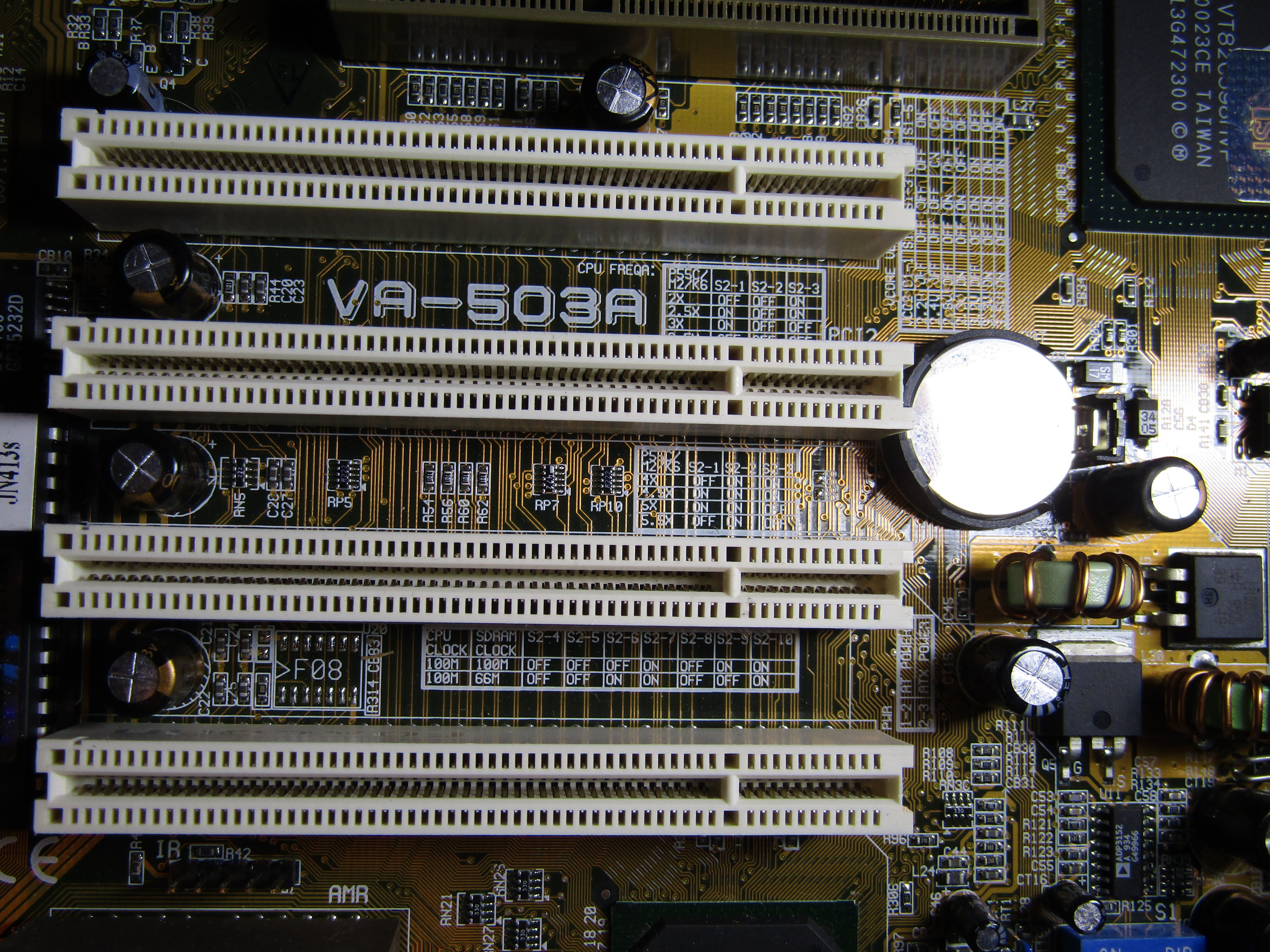
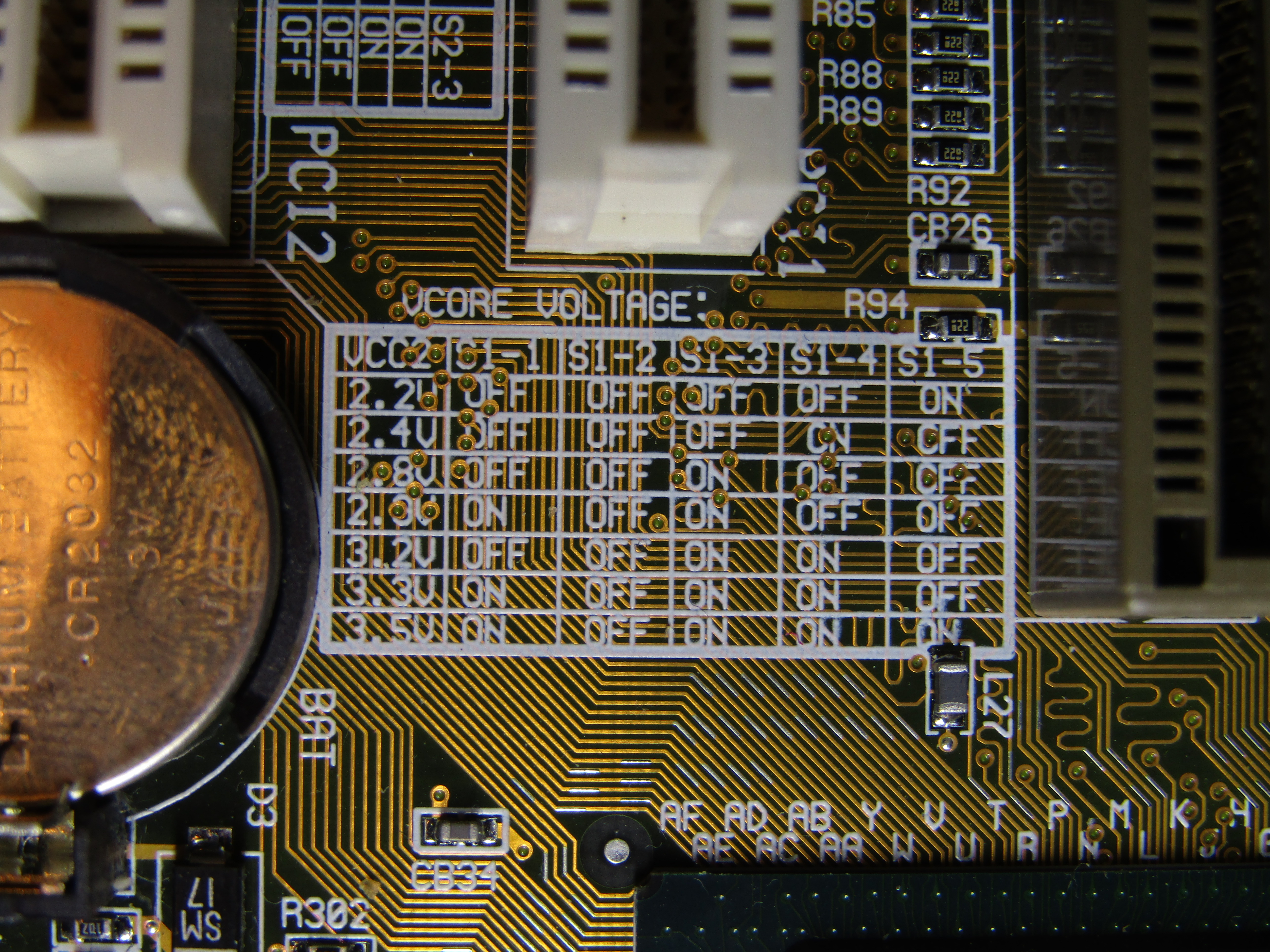
The board accepts Socket 7 type processors, which allowed it to support a wide range of processors, including Intel’s Pentium & Pentium MMX, Cyrix/IBM M, MX, & L models, and AMD-K6, which is what I used during this build (you’ll see later). To enable support for such a wide range of speeds and voltages, there are two sets of dip switches to specify CPU Vcore voltage, CPU/DRAM frequency, and the ratio of CPU freq. to Bus freq.
This board really takes some manual work and careful reading to get everything working compared to modern motherboards, which have ability to figure everything out themselves through careful design and other improvements in the last 20 years. Luckily, even if you don’t have the manual, the dip switch settings are printed on the motherboard as seen in the photo above and here:
Beyond configuration, the motherboard has a lot of useful slots, plugs and ports that give ample room for expansion and customization. I liked how it gave the user an opportunity to easily customize the PC with a full range of expansion slot types to support plenty of different cards.
Slots
4 32-bit PCI bus slots
These are the primary slots of the board, and should be familiar to anyone who has built a PC in the last 2 decades. These 5v 32-bit PCI slots can operate at either 33 or 66 Mhz, but I wasn’t able to find any info in the manual about these specifically. Given the release data of the motherboard, these slots are probably either PCI 2.1 or 2.2.
1 16-bit ISA bus slot
This slot architecture was originally designed in 1981 as part of the IBM PC project. Despite being replaced by PCI, it was kept on motherboards to allow users to use much older hardware that they already owned from other computers. I had an old IDE controller card that would have fit in this slot, but I opted not to use it as I believe it was a 32-bit ISA slot and I didn’t have any additional hard drives I was dying to add to this build.
1 32-bit AGP bus slot
This slot is a dedicated slot for a graphics card. Today PCI-e is primarily used, but this was an architecture that came slightly before. This bus was designed specifically for graphics cards, having a direct line between the bus and the system memory, separate from the PCI bus. It operated in two modes: 1x (66MHz) and 2x (133MHz) and had higher bandwidth when compared to the 32-bit PCI bus, which operated at 33MHz/66MHz.
This allowed for higher clock speeds and less contention with other PCI devices. The AGP spec is heavily based on PCI, with the AGP bus being designed as a super set of the conventional PCI bus.
One interesting thing about the design on the AGP bus was the addition of what’s called Sideband addressing, which allowed the cards to separate the address and data buses so the address uses a separate set of pins than the data, allowing for faster data throughput.
Having faster access to data also allowed cards to directly use textures from ram instead of needing to copy the textures onto the cards memory first.
1 AMR bus slot
AMR stands for Audio Modem Riser, and interfaces with, you guessed it, audio and modem expansion cards. It is a dedicated bus that runs on top of the PCI bus. Here is the specification for the slot from September 1998: link. One shortfall of this bus was how it didn’t allow for hardware acceleration on the card. It seems the reasoning was to have the card integrate with the motherboard at a high level, allowing for cheaper implementation cost of the expansion card and slot on the motherboard. The card didn’t even need to be a riser card, it could be directly soldered to the board. The cards were to support the AC/MC/AMC ‘97 specifications1 and contain one or more codec on the card to support the different configurations.
On page 10 of the specification, you can see how hardware acceleration is only allowed on the motherboard side, not the card.

The spec specifically says “The AMR architecture does NOT support aftermarket audio or modem upgrades by only changing the AMR module.”, further specifying that all hardware-accelerated controllers need to be designed as part of the motherboard, not part of the expansion card. This meant if you wanted to upgrade the audio or modem card then a you would need to use either a PCI bus expansion slot or a USB port to install a card with more power. It’s no surprise that this slot was later supplanted by PCI when adding a audio or modem card.
Infrared IrDA connector
IrDA stands for Infrared Data Association, which is an industry group that created a set of wireless infrared communication protocols. IrDA also refers to that set of protocols. It uses infrared to communicate data between devices. Uses included a wide variety of payload types, such as networking (IrLAN), parallel/serial communication (IrCOMM), data transmission (IrSimple and IrSimpleShot), and object exchange (OBEX).
I don’t have any IrDA compatible hardware, so sadly this connector will remain unplugged.
Connectors and Ports
Here’s a quick summary of the remaining bells and whistles present on the board.
IO Headers
- AT Keyboard port
- 2 serial ports
- 2 usb headers
- 1 printer connector
Drive Headers
- 1 Floppy Disk Drive
- 2 IDE HDD connectors
Power
- 1 ATX power connector -
- 1 AT Power connector - can see why atx is better
- 1 Remote Power connector
Fans
- 1 CPU fan connector
- 1 chassis fan connector
Front Panel Headers
- IDE LED - Blinks when hard drives are activated
- Speaker - For the case speaker
- Reset Button - Use to reboot instead of using the power switch
- Suspend Button - Tells OS to suspend (?)
- Power LED - Indicates when the system is on/off
- Remote Power Button - Turns the system on and off instead of using the switch on the power supply
- Message LED - Controlled by OS or Application software
- Chassis intrusion alarm -
Processor: AMD-K6-2
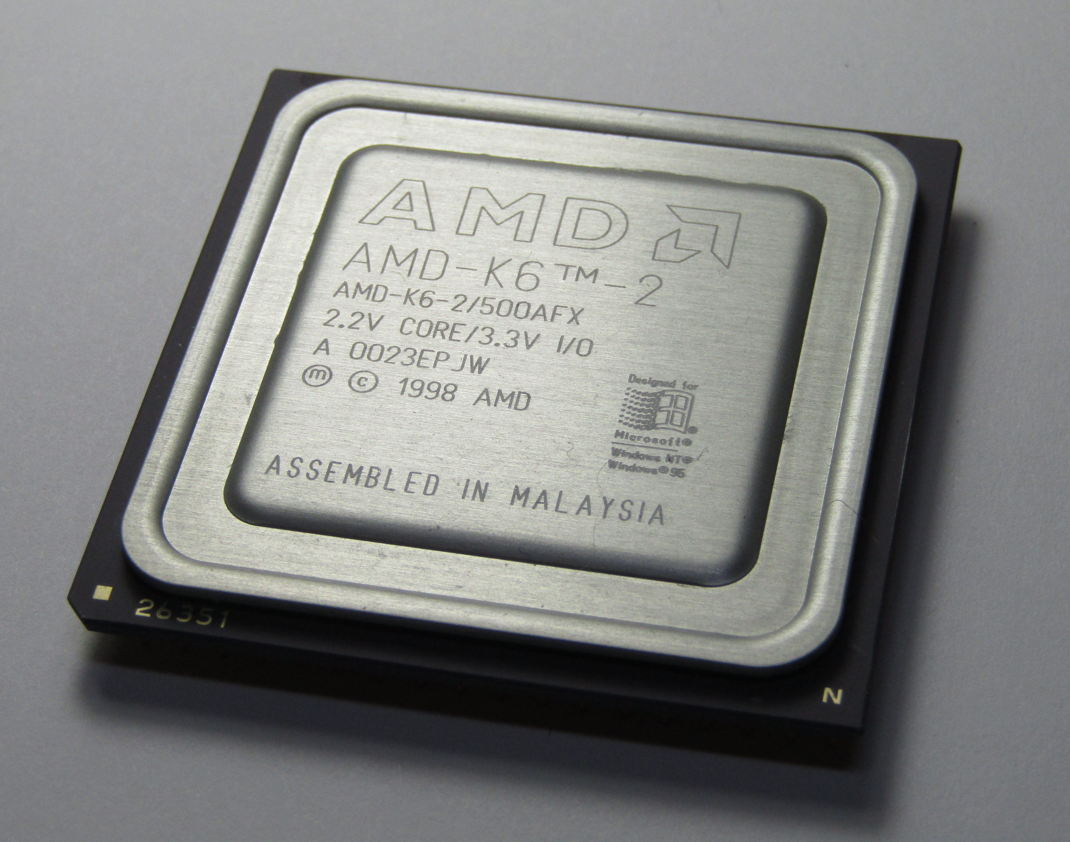
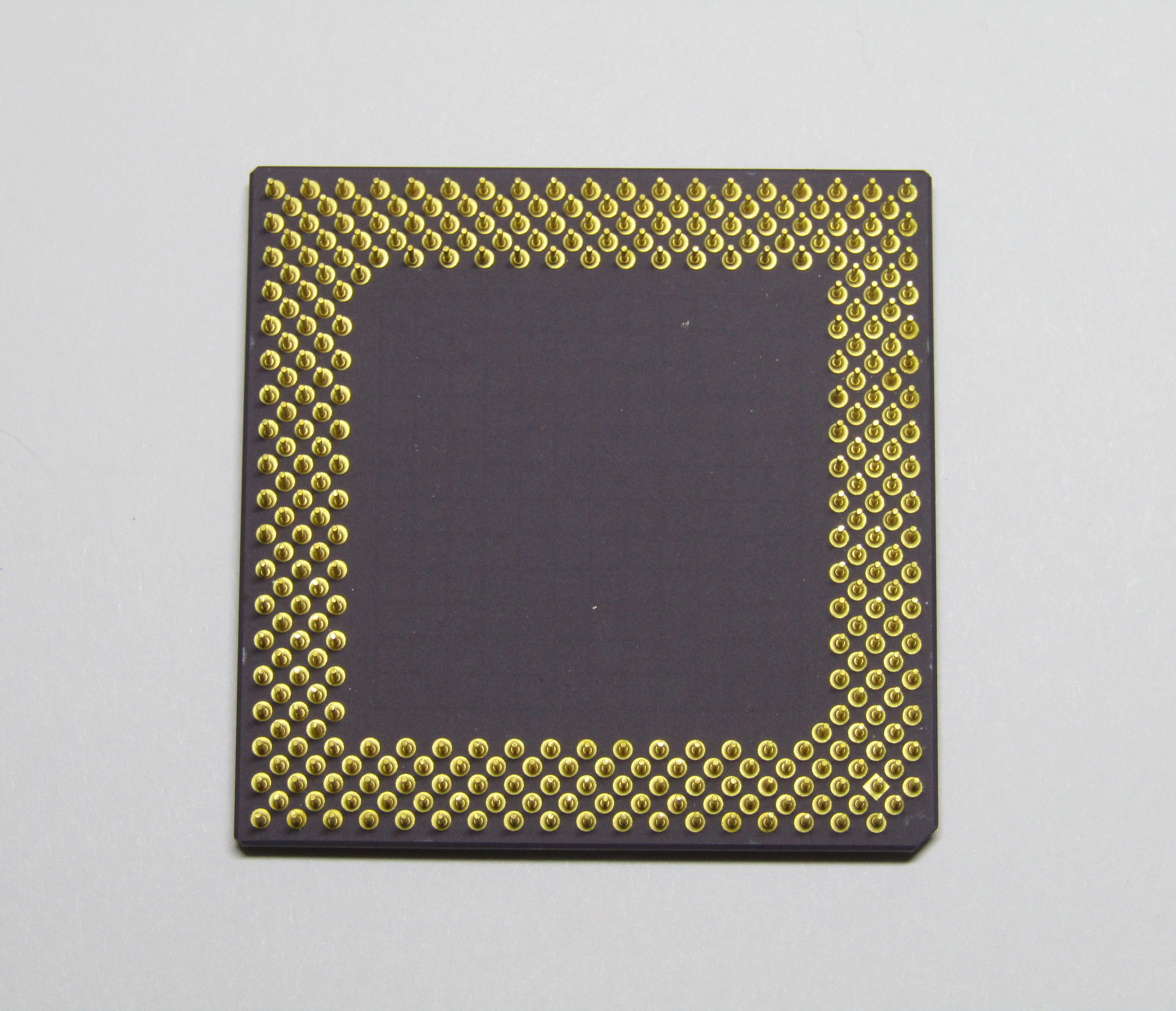
Text on processor:
AMD
AMD-K6™-2
AMD-K6-2/500AFX
2.2 V Core/3.3 V I/O
A 0023EPJW
Ⓜ © 1998 AMD
ASSEMBLED IN MALAYSIA
This processor was released in May 1998 as a competitor to Intel’s Pentium II. It was preceded by the AMD K-6 in April 1997 and succeeded by the AMD-K6-III in February 1999. This is the Chomper Extended (CXT) model, sporting a 500 MHz clock rate
In an attempt to compete with Intel’s floating point instruction speed, this was the first processor to include SIMD instructions, called 3DNow! by AMD.
This allows the processor to perform arithmetic operations on a set of registers at the same time, instead of having to perform the operation on each register individually.
The processor footprint was designed for Super Socket 7, but it was backward compatible with Socket 7 by preserving the same pin layout. The motherboard we’re slotting it into is equipped with a regular Socket 7.
Specs: CPU-World
RAM
For this build I was able to dig up 3 different sticks of SDRAM.
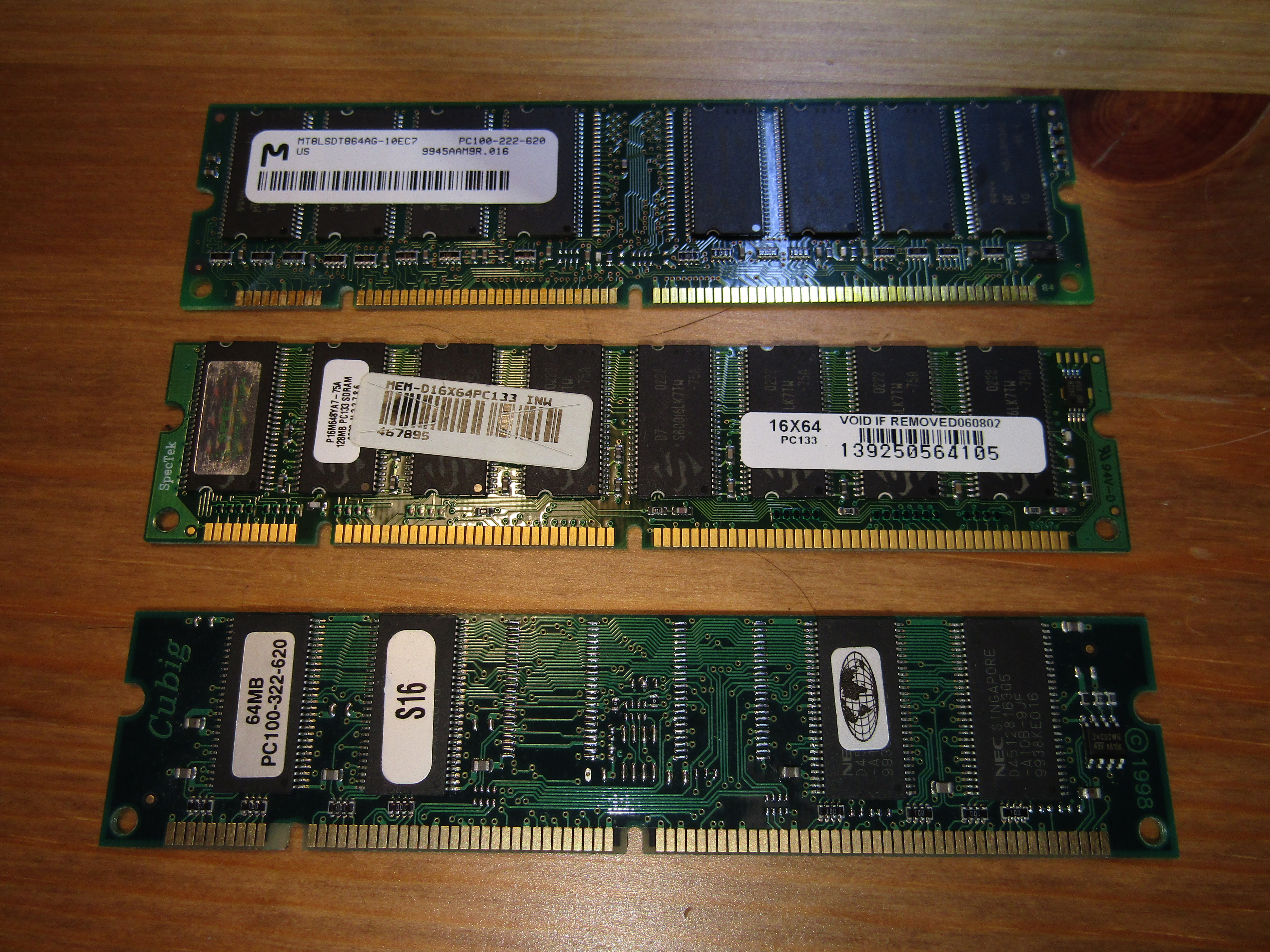
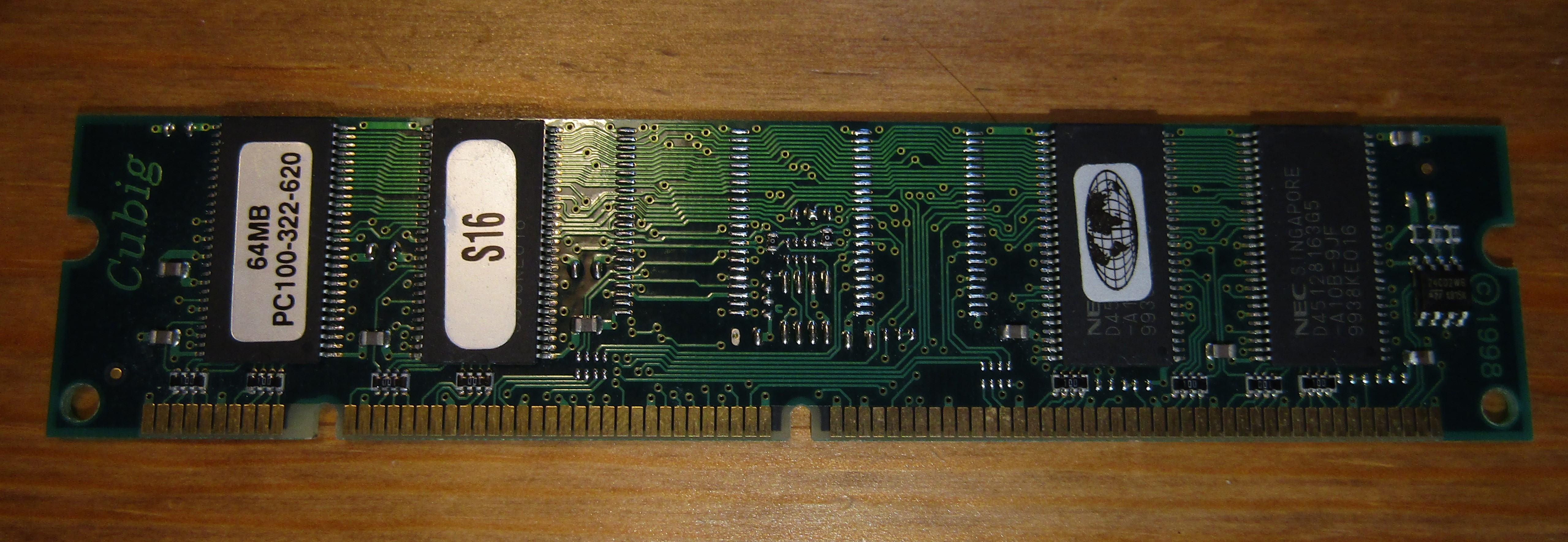
- 64MB - Cubig PC100-322-620
- 64MB - Micron MT8LSDT864AG-10EC7 - PC100-222-620
- 128MB - SpecTek P16M648A7-75A - PC133-3??-6?0
Each stick of RAM’s type is identified by the PCX00-XXX-XXX. The PC100 and PC133 describe the timings of the sticks. Motherboard is designed for 100MHz DIMMs, so the 128MB potentially would have been incompatible. PC133 is listed as backwards compatible with PC100, so the DIMM may have worked despite the difference (if the motherboard was functional).
The next number (322 or 222) describes more characteristics of the DIMM. The first number describes the DIMM’s Column Address [Strobe|Select] or CAS latency, or tCL. This refers to the number of clock cycles it takes for data to become available when a READ command is registered. The latency is based on the clock rate, not the processor cycles. If you look at the table of memory timings on the CAS wikipedia page (located here), you can see that CAS latency values have actually been rising, while the cycle times have decreased. That and other advancements in memory technology have made modern memory much faster and more responsive than these SDRAM sticks.
The next two numbers describe the tRCD and tRP are additional sources of latency. tRCD describes the latency to convert a Row address to Column address Delay. This is the time it takes for a row to be selected, which must be done before accessing the columns of the row. When multiple access take place on the same column of data, this delay won’t be present.
The tRP stand for Row Precharge time, which is the amount of cycles it takes for a newly selected row to become available. This is only a factor when a different row is selected. When a different row is selected, the total time it takes for the data to become available will be tCL+tRCD+tRP.
The final number in the identifier (620). The first digit is the ACcess time from the CLK positive edge, tAC. The second digit has something to do with the Serial Presence Detect functionality, or SPD. This is a small (~128 Bytes) area of memory that stores properties of the RAM module. The final digit is a vendor specific value, with witch to store a version or other specific number.
Now with that background, I’ll now go over the characteristics of the three sticks.
Cubig 64MB PC100-322-620
Micron MT8LSDT864AG-10EC7

Datasheet: https://www.datasheets360.com/pdf/-5710319829756231807
This make of memory has a few different models, ones that support 66MHz, 100MHz and 133MHz clock frequencies.
This model, 10EC7, is 100MHz with a CAS of 2.
SpecTek P16M648A7-75A
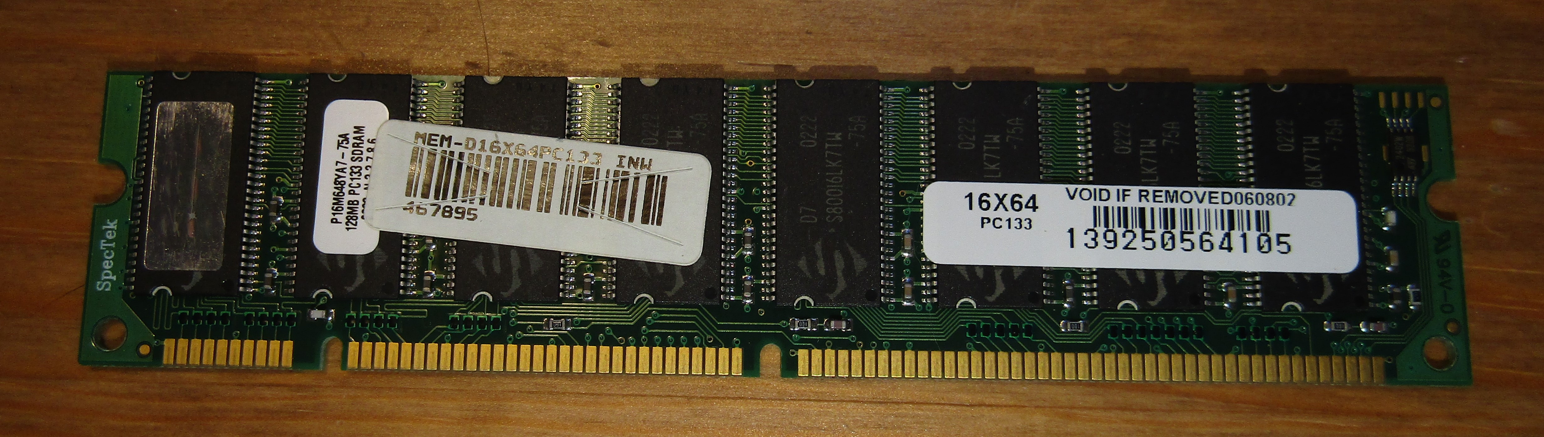
Datasheet: https://www.spectek.com/pdfs/16M_648YL.PDF
This DIMM supports both 100MHz and 133MHz clock frequencies.
Drives
Disk Drive
Model #: BCD F560A
52x Max
Just a standard disk drive. It has a headphone jack in the front, which allowed a user to listen to sound through the disk drive. This was popular during a time when not all computers contained a sound card or hardware to process audio. Adding the capability to the disk drive allowed a user not only to play sound from the computer, but also play media files present on inserted disks without any assistance from the rest of the computer (besides power). This model of disk drive is especially fancy, not only possessing an 1/8” audio jack port but also a volume wheel, a play/skip button and a stop/eject button.
It also came with a cable, allowing it to be linked it to sound card to receive analog audio from the rest of the computer.
3 1/2” Floppy Disk Drive
Mitsumi
Model D359M3
Normal floppy disk drive I like the stamped Company name on the case.
Hard Drive
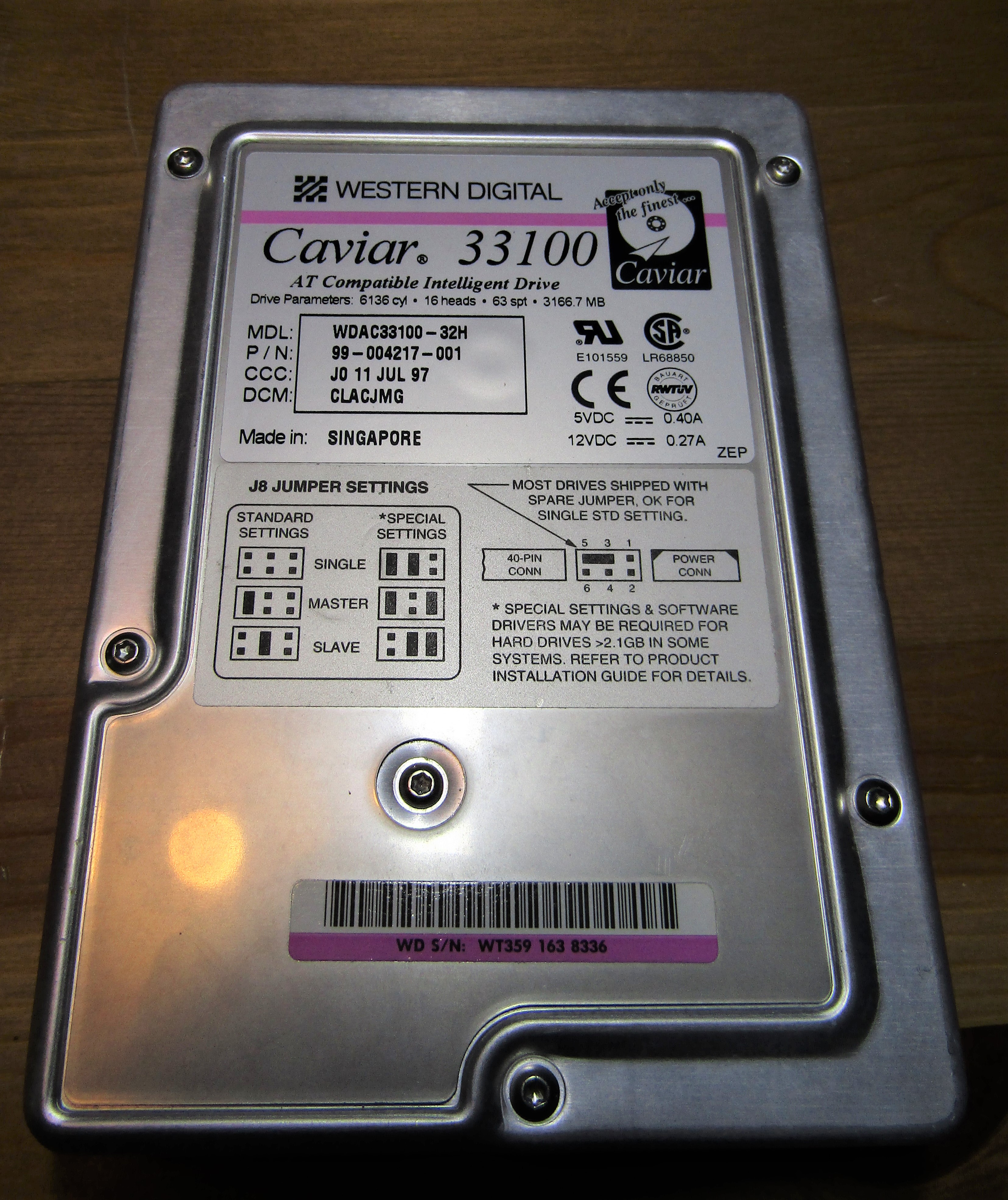
The hard drive that came with the computer is a Western Digital Caviar 33100. It was produced on July 11, 1997 in Singapore. It’s a 3166.7 MB drive with a PATA 40 pin connector. It also has jumpers, allowing you to set the drive as a single, master, or slave drive.
Though it’s not the most useful drive these days, I like the purple highlights that remind of the vaporwave aesthetic.
More information about this drive model can be found here.
Cards
Sound Card
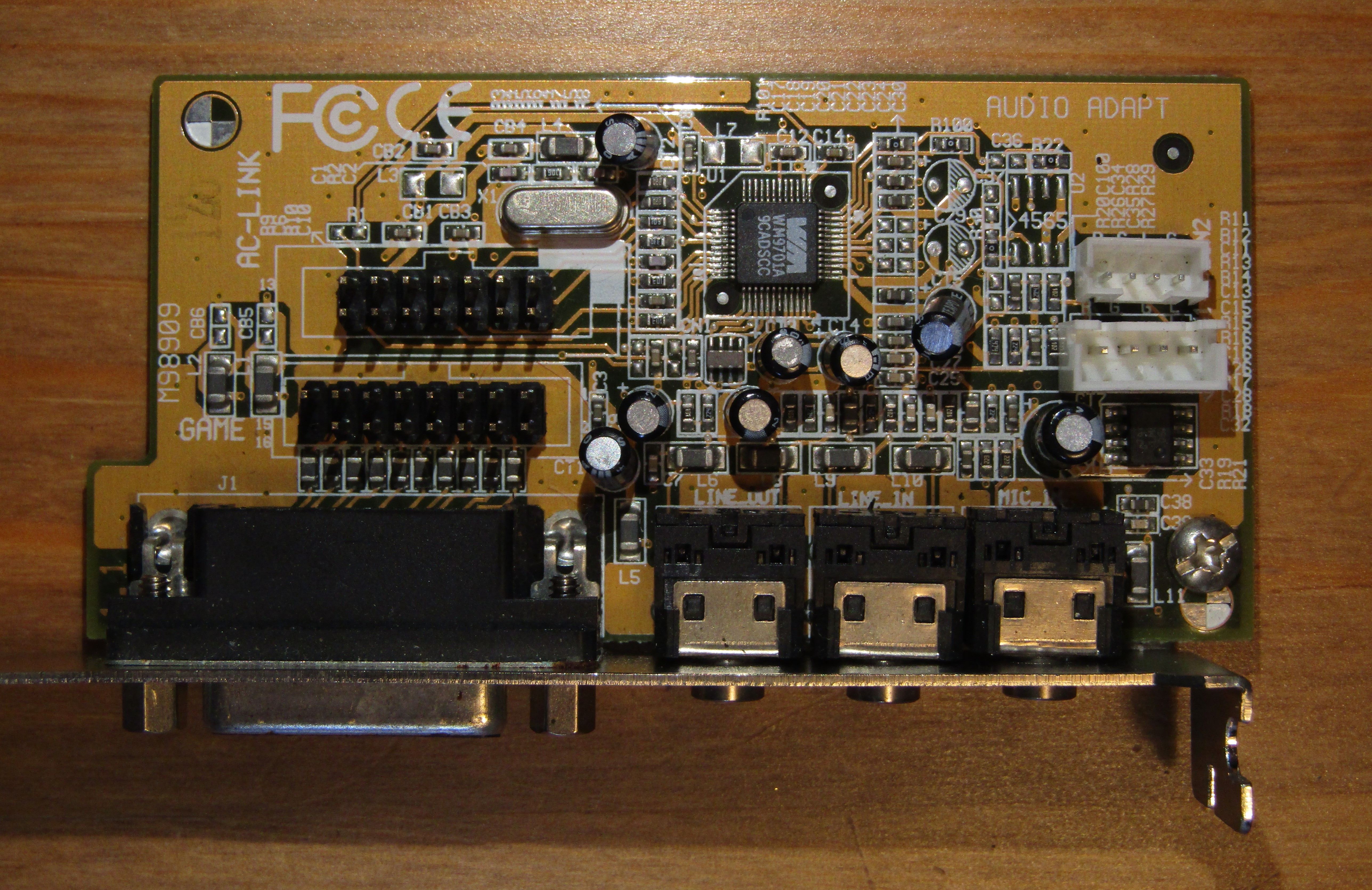 Chip text:
WM
WM9701A
9CADSCC
Labeled as an audio adapter
- Line out
- Line in
- Microphone
- AC-97 link
- Game port
The line in, line out and microphone allowed one to plug in their sound equipment. Besides those ports is a 15 pin game port that was used for game joysticks and sometimes midi devices. Since video games required a sound card to produce better sound that bleeps and bloops, the game port was included on many sound cards starting with the first Sound Blaster in 1989.
This card also includes two additional plugs that allow you to plug the CD-ROM drive into the sound card. Then when a music cd or a cd with readable sound files was inserted into the drive it could be played from the drive, without needing to install and run a program on the computer itself.
M98909 (?)
Video Card
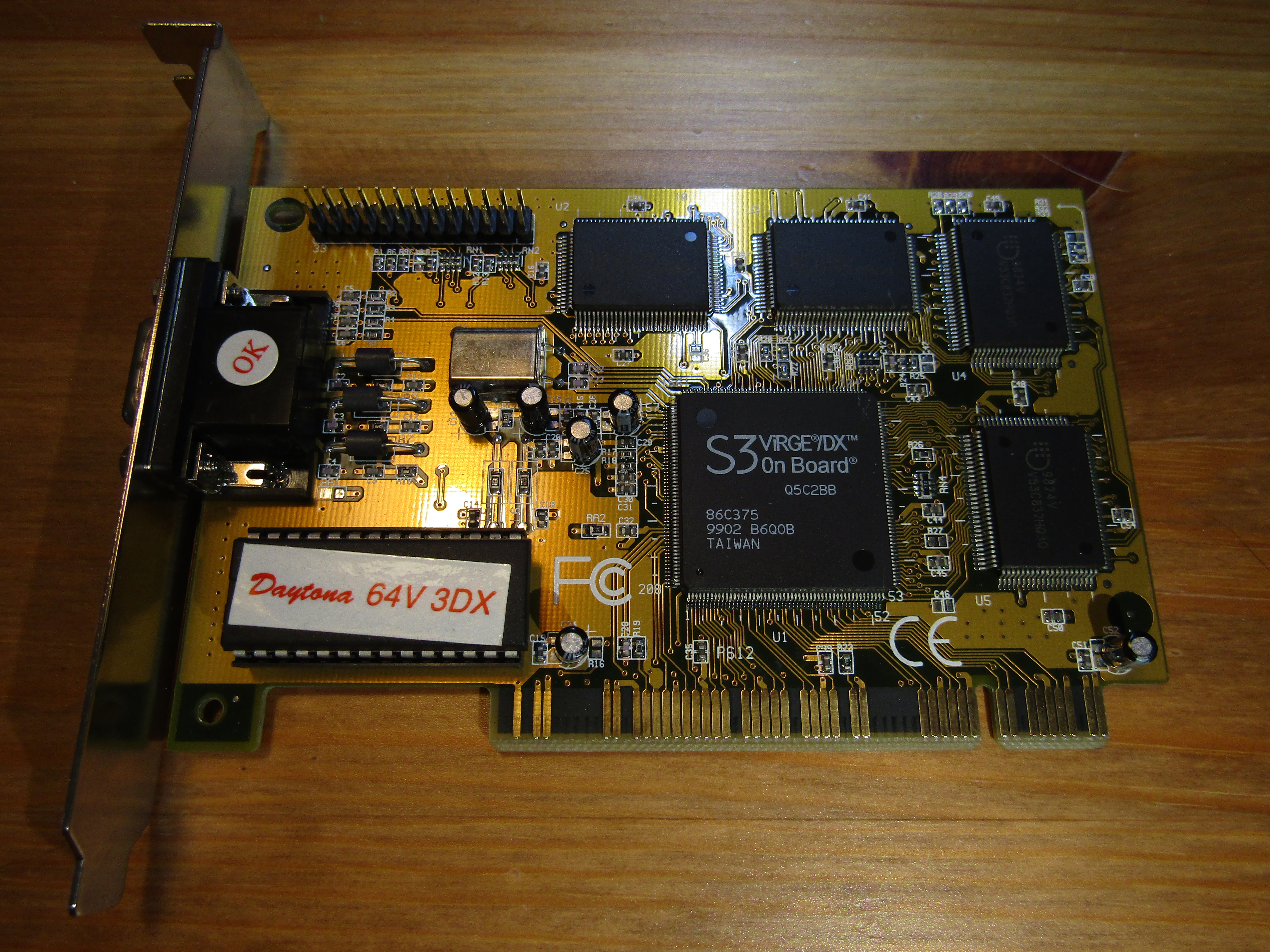
Daytona 64V 3DX
Main chip:
S3 ViRGE/DX
On Board

Q5C2BB
86C375
9902 B6Q0B
TAIWAN
64 bit 2D/3D graphics 170Hz
“DX” means equipped with dram
supported 1280/1024 75Hz w/ 256 colors
Surrounding memory chiplets:
4x
9824V
V53C832HQ30
EDO DRAM 5V EDO stand for “Extended data out”, which means that the data output from a previous access cycle remains available during a new access cycle. This allows for improved performance through overlap in operations (pipelining).
8388608 bit memory density
Organization 256K/32
Ethernet Card
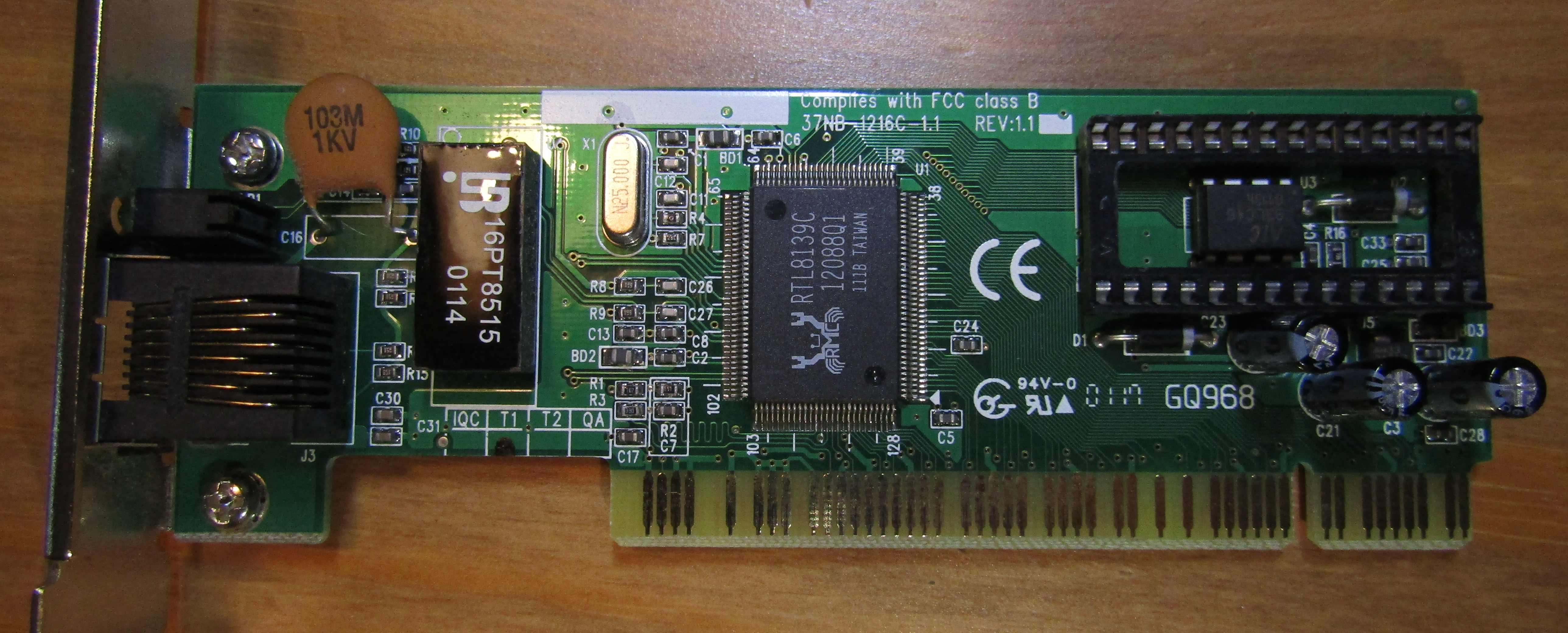
Board Identifier: GQ968
Main chip text:
RTL8139C
12088Q1
111B TAIWAN
This ethernet card hosts a Realtek RTL8139C chip, boasting 10Mbps and 100Mbps operation, Wake-On-Lan functionality, separate 2KByte Rx and Tx stacks (FIFO), and built in PCI support. It is able to support two types of 802.3 standard, 802.3u and 802.3x.
The 802.3 standard is a IEEE standard that defines physical and data link layers (MAC). 802.3u was introduced in 1995, and supports three types of cables that transfer data at 100Mbps (12.5 MB/s) speeds along with auto-negotiation for the connection. One of the types, 100BASE-TX, we still use today. It consists of two twisted pairs, and is better known as Cat-5, Cat-5e, Cat-6, and Cat-7, though at the time this card was made it would have only used Cat-5.
The second type, 100BASE-T4, uses the Cat-3 type cable, which is usually used as telephone wiring. The final type support is 100BASE-FX, which is a version of ethernet that operates over optical fiber. Despite the chip supporting it, I don’t believe it would have ever been used on this card.
The other standard, 802.3x describes ethernet flow control, which defines a “pause” frame. When one device is sending data to another device, pause frame is usually sent by receiving device to request that the sender temporarily halt sending packets. This is useful in cases where the sending device is transmitting data faster than than the receiver can accept.
Using this chip as an example, it would send a pause frame when the 2KByte Rx buffer was filled.
If the sender continued to transmit data, our chip would have to drop the data and most likely require that it be retransmitted.
By sending the pause frame, our chip communicated two things: that transmission to the receiver should temporarily halt, and a 2 byte number defining the length of time transmission should halt.
The pause length is measured in units of pause “quanta”, where each unit is equal to 512 bit times, witch is the time it takes for one bit to leave the NIC.
In our case, our (maximum) NIC speed is 100Mbit/s, so sending a pause frame would pause the transmission of data for 1 / (10 * 10^7) * 512 => 5120 Nanoseconds.
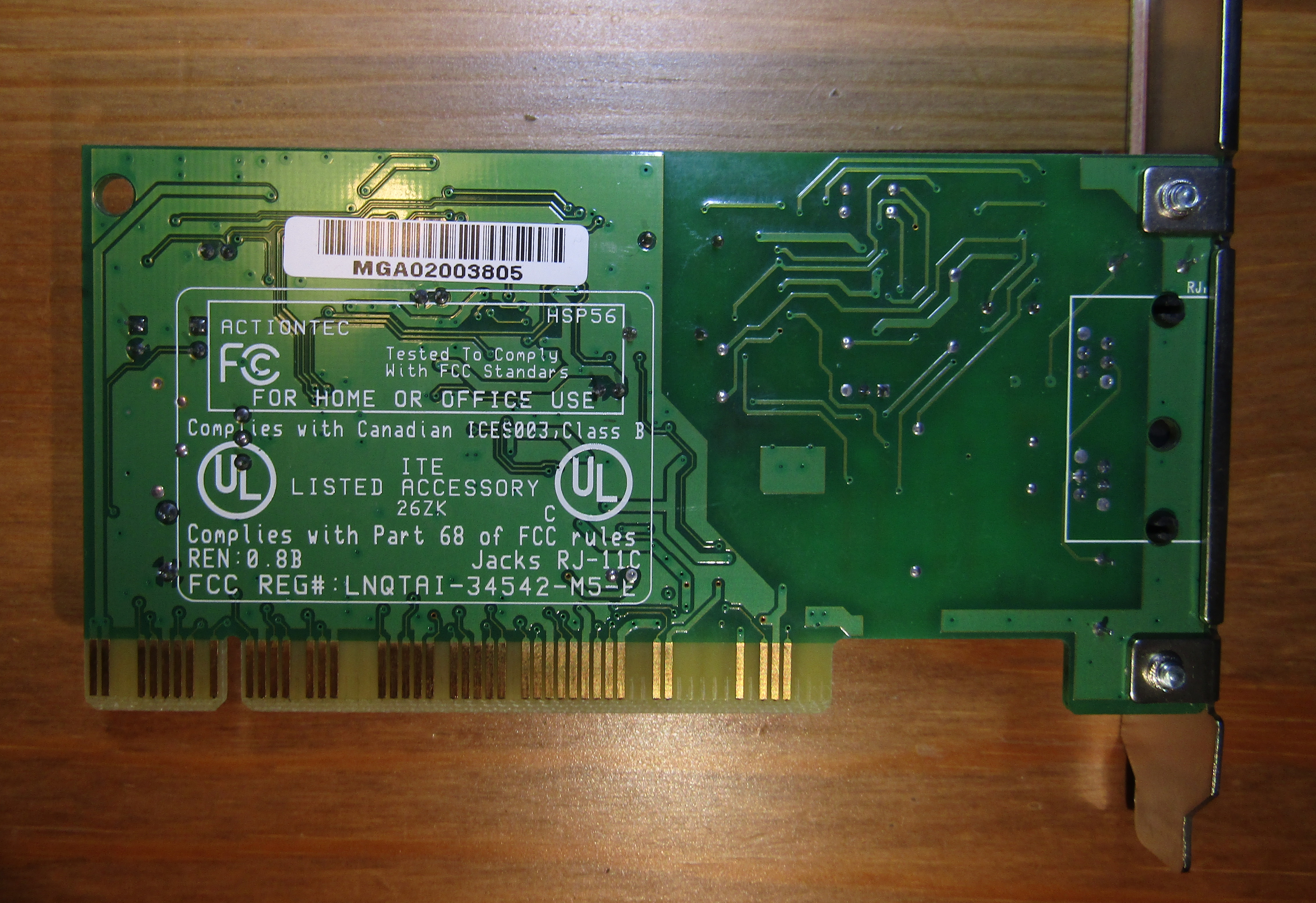
Dial up card
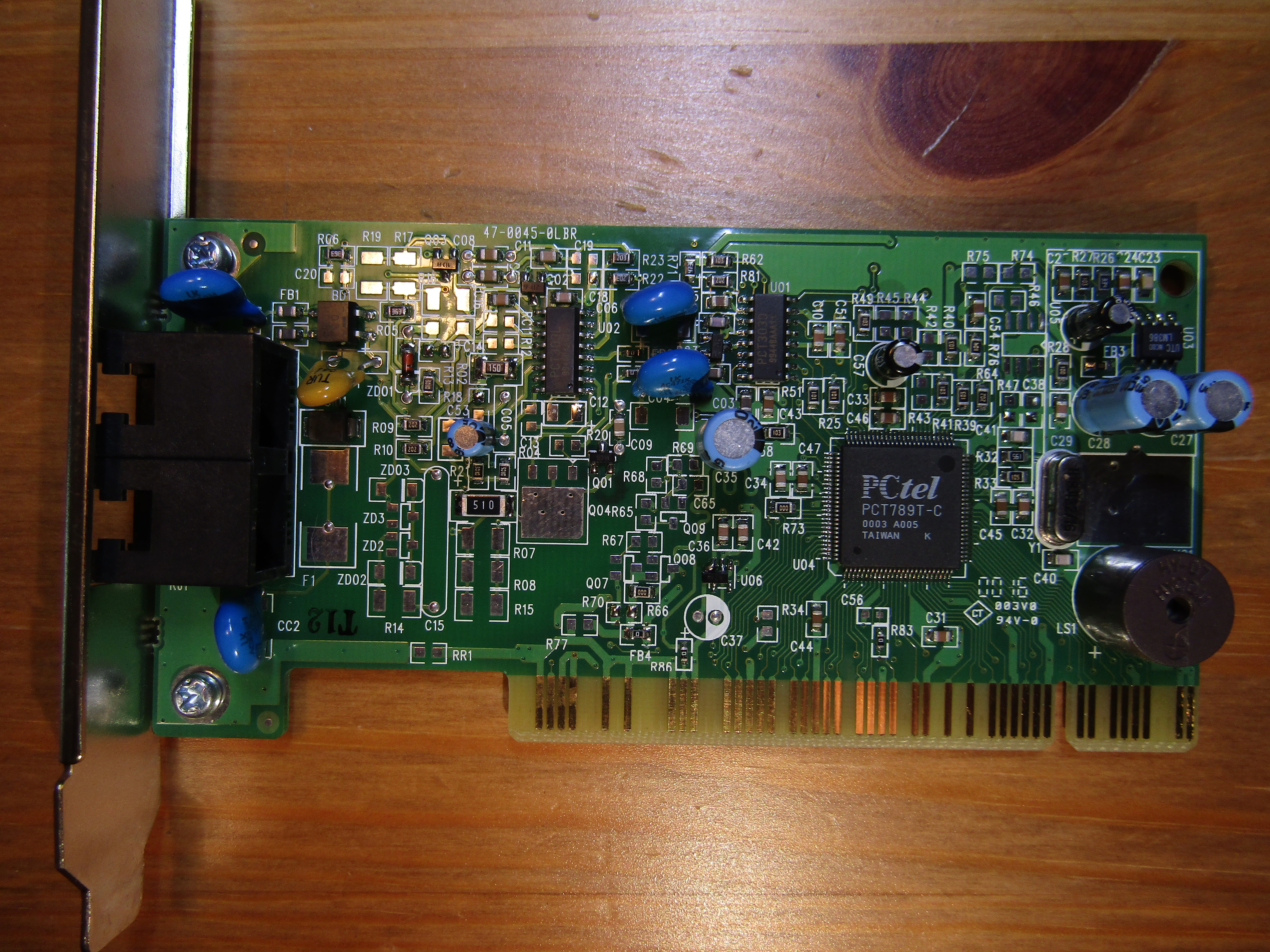
Main chip text:
PCtel
PCT789T-C
0003 A005
TAIWAN K
Actiontec branded on the back, no part identifier. Searching for the PCtel chip online led me to it’s datasheet, linked above. The card I have here is extremely similar to the card displayed in the datasheet, with only a few differences.
This is a standard (for the time) modem that is placed in the PCI slot of the motherboard. It supports up to 56K speeds, in addition to H.324 video conferencing and various fax modulation protocols. It is listed as supporting Windows 95, Windows 98, Windows NT, Win CE 2.0, and Linux.
USB Card
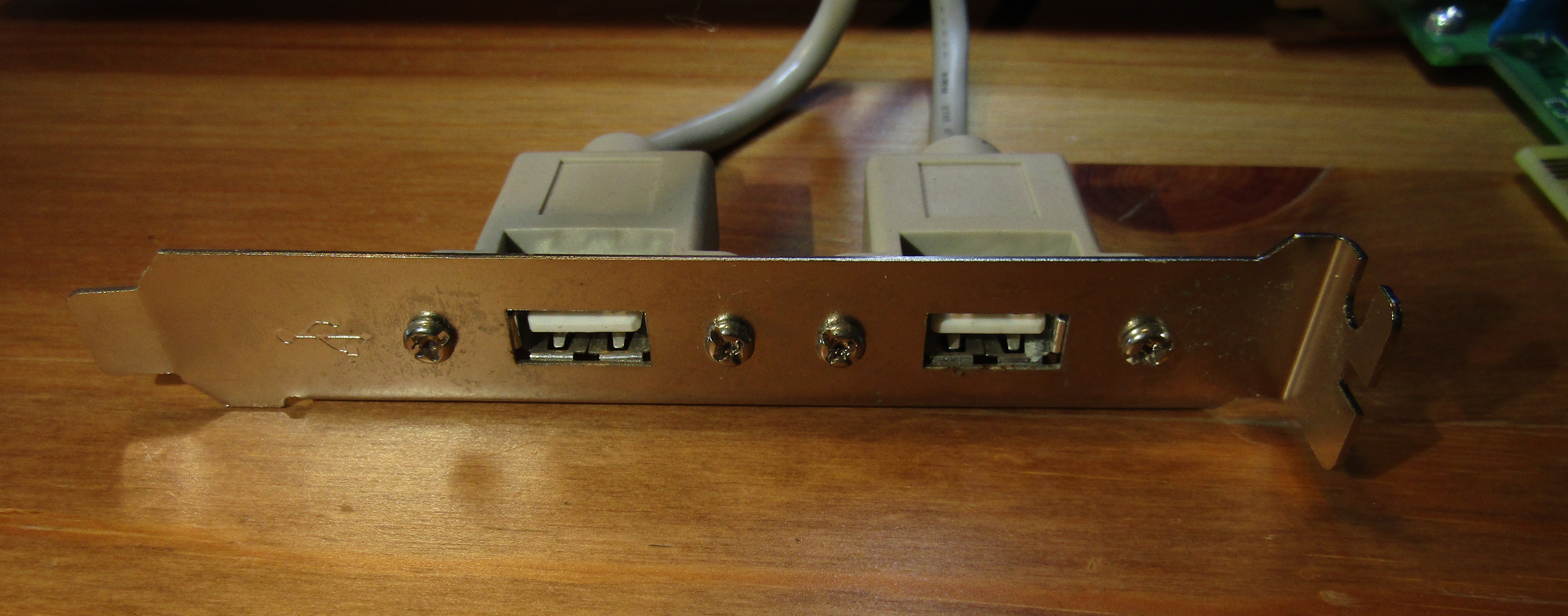
A breakout panel hosting two separate USB ports. It connects via a single cable to the motherboard. It may still be able to be used on a modern PC, as the cable pinout is the same as is still used today (at least for USB types <3.0).
I/O Card
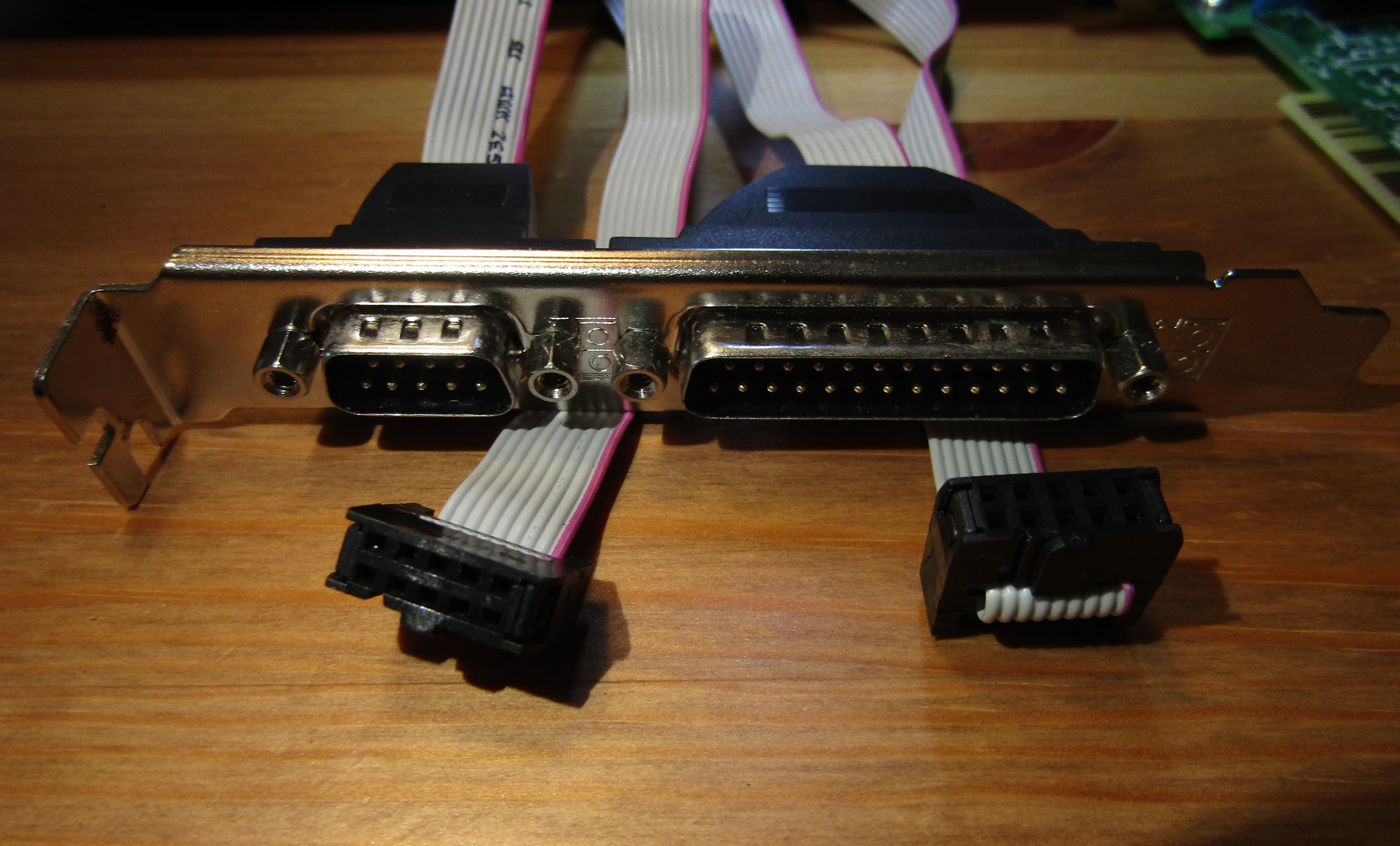
Simple D-sub male connector panel, to be plugged into the motherboard. It possesses a DE-9M connector and a DB-25M connector. The smaller 9 pin port could be used for game controllers, while the larger one could be used as a parallel port, often connected to a printer.
These are very common ports, and have even been used on game consoles like the Atari 2600 and Sega Genesis.
Footnotes
-
AC: Audio Codec, MC: Modem Codec, AMC: Audio/Modem Codec. ↩