Gameboy DMG ROM and RAM Bank Switching
22 Jul 2019 | 13 minutes to readBank switching is a method of switching what data is accessible by a program.
It was used to allow a CPU with a static memory map the ability to address additional data than what would usually be able to be addressed.
The original Gameboy DMG used a CPU similar to the Zilog Z-80.
It used a 16 bit address bus, allowing it to access up to 2^16 bytes ($0000-$FFFF).
Here is an image of the memory map for the Gameboy, sourced from Pan Docs.
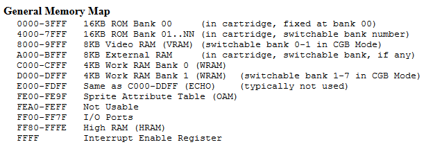
ROM and RAM bank switching is controlled by a memory bank controller present on the cartridge. By writing values to areas of read-only memory, a game or program is able to specify which ROM banks to access when read operations are performed.
The simplest cartridges simply contained ROM and had only had 32 KBytes of space.
It is mapped directly to $0000-$7FFF.
There was no MBC on these types of cartridges because the entire game would be able to fit on the cartridge.
This types of cartridge could also contain up to 8KB of RAM, mapped to $A000-$BFFF, though it would require an MBC-like circuit to work.
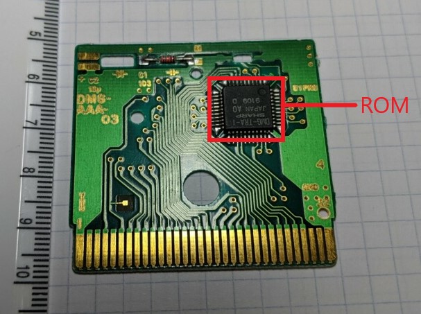
An example of a game that didn’t use a MBC was Tetris, whose ROM is only 19KB. The game was small enough that no bank We can see here how simple the game cartridge is, only requiring the ROM chip with the game code. Cart Information
Larger games required larger amounts of storage which the Gameboy was not natively able to address. Bank switching is the solution to this.
Cartridges needing additional capabilities had a lot more going on than Tetris. Instead of data lines connecting directly to the ROM, they instead go through a memory bank controller that manages manages the bank switching of the ROM and RAM through intercepting read and write commands to certain addresses.
Types of Memory Bank Controllers
There were 4 (and a half) types of MBCs that cartridges used. They each possessed different amounts of ROM and RAM. Each ROM bank was 16KB in size
- MBC1: max 2MB ROM (125 banks) and/or up to 32KB RAM
- MBC2: max 256KB ROM (16 banks) and 512x4 bits RAM
- MBC3: max 2MB ROM (128 banks) and/or 32KB RAM (4 banks) and Timer
- MBC5: max 8MB ROM (512 banks) and/or 128KB RAM (16 banks)
- HuC1: Similar to MBC1 with an Infrared Controller
One thing to note is that MBC1 and MBC3 both support 2MB, but have a different number of banks (125 vs. 128). I will explain that once I explain the memory map and bank switching. In this article, I primarily focus on explaining how the MBC1 works.
MBC1 Memory Map
This was the first MBC chip for the Gameboy. It behaves much the same as the other, with a few exceptions. A cartridge with an MBC1 uses to following memory ranges:
$0000-$3FFF: ROM Bank $00 (Read Only)
This always contains the first 16KB of the cartridge, the first memory bank. It is unable to be switched or modified.
$4000-$7FFF: Additional ROM Banks (Read Only)
This area of memory will contain whatever memory bank is currently selected.
$A000-$BFFF: Ram Bank, if present (Read/Write)
This is where RAM banks will be placed in memory. They are able to be both written to and read from, allowing the game to store data. If the cartridge contains a battery, like in Pokemon cartridges, the data written is able to be preserved across shutdowns. This type of MBC had 3 different RAM options:
- 2KB:
$A000-A7FF - 8KB:
$A000-BFFF - 32KB:
$A000-BFFF(four switchable 8KB banks)
$0000-$1FFF: RAM Enable (Write Only)
Before a game is able to use the RAM, it must be specifically enabled.
This is done by writing a value with the lower 4 bits being $0A somewhere in this address space.
To disable RAM, any number except $0A can be written.
It does not matter where it is written, just as long as it within the address range.
You will notice that this address range is part of the first ROM bank, which is read only.
Because it is ROM, there is obviously no way to actually write data to those memory locations.
Instead, the write call is “intercepted” and interpreted differently by the MBC.
This method of writing to ROM is also used for the remaining memory areas I’ll explain now.
$2000-$3FFF: ROM Bank Number (Write Only)
Writing a value to this address range will select the lower 5 bits of the bank number.
There are a few special cases though.
If the value $00 is written, it will converted to bank $01.
This is not an issue because bank $00 is always present at $0000-$3FFF.
The issue lies in writing the values $20, $40, and $60.
When these values are written, instead of addressing the correct ROM banks they will address banks $21$41 and $61 respectively.
I couldn’t find an explanation of why this takes place, but I assume it has something to do with how the lower 5 bits are used when choosing the bank.
Each of these numbers have all zeros as the lower 5 bits (0x0XX00000).
This issue is not present in MBC2 and MBC3.
$6000-$7FFF: ROM/RAM Mode Select (Write Only)
Writing either $00 or $01 to this area will select which mode the MBC is in.
On an MBC1, there are two modes: 16Mb ROM/8KB RAM and 4Mb ROM/32KB RAM.
The game is able to switch between the modes on the fly, allowing a game to access extended ROM banks during normal operation and switch to RAM mode temporarily when data needs to be read.
Valid values are $00 for ROM mode and $01 for RAM mode.
$4000-$5FFF: RAM Bank Number or Upper Bits of ROM Bank Number (Write Only)
Writing to this area of memory will effect the ROM or RAM modes, depending on what is written in $6000-$7FFF.
Only the first two bits of the value matter.
If in ROM mode (no RAM bank switching), it will specify the upper two bits of the ROM bank number.
In this mode, only RAM bank $00 may be used.
If in RAM mode, it will specify which RAM bank to load into $A000-$BFFF.
In this mode, only ROM banks $00-$1f may be used.
The MBC1 is only able to switch between 125 different ROM banks, instead of the expected 128.
The ROM banks are addressed using a 6 bit number created from writing to $2000-$3FFF and $4000-$5FFF.
The reason is because of the number conversion when writing $20, $40, and $60 to $2000-$3FFF.
This results in it being able to address 128-3 or 125 banks for a actual total of 1.95MB, not 2MB.
This issue is not present in MBC2 and MBC3.
MBC2 has a maximum of 16 banks, so the issue is never encountered.
The MBC3 chip correctly addresses $20, $40, and $60 and does not perform the conversion.
Bank Switching in Practice
That was a lot of numbers and memory ranges, so now I’ll give a few examples of bank switching and the process a game would take.
When the Gameboy is first turned on, the cartridge header is read and gives information on the ROM and RAM sizes present on the cartridge.
Byte $0147 specifies the type of MBC and what hardware is present on the cart.
Byte $0148 specifies the size of the ROM, from which the number of banks can be derived.
The next byte after, $0149, specifies the size of the RAM
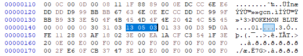
Looking at a compiled ROM of Pokemon Blue, we can see that the MBC type is $13 and the ROM banking type is $05.
These values correspond to different hardware settings, which we can see by referencing the header definition.
Looking these values up against the table, we can see that the MBC type is MBC3+RAM+BATTERY1 and that there is 1MB of ROM, or 64 banks.
We can further verify this by checking the size of a dumped ROM, which is exactly 1024KB.
Finally, the RAM size value is $03, which corresponds to 32KB of RAM, 4 banks of 8KB.
We can further verify these values by looking at the actual hardware of Pokemon Blue. Once again, we have the picture of the PCB of the game here:
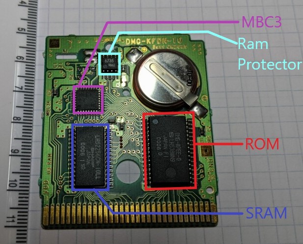
The MBC chip, highlighted in purple, is labeled as an MBC3 chip. Below that, we have the SRAM in blue, the the ROM chip is red to the right. Since it has the MBC3, RAM chip and a battery, we can confirm that the MBC type value is correct.
The SRAM chip is a 256K LH52256CN-10LL (Datasheet). This is where the game save resides when the game is not being played. This chip contains much more SRAM than the cartridge header specifies oddly enough. I was unable to determine why. The data is preserved in the chip by using the coin battery to make sure the SRAM always has power. The RAM protector manages the power going into the SRAM from the battery, allowing the data to be preserved. Cart Information
The later generations of Pokemon (Gold/Silver/Crystal) were similarly designed, but suffered from battery issues sooner than Red and Blue. This was because these games had an internal clock that kept the time. You can see the pads where it would be soldered on the PCB above in the upper left corner. This additional power draw meant that the battery needed to be replaced much sooner, resulting in saved data being lost.
For these examples I used the Pokemon Red/Blue disassembly located on Github. It is very well commented and not to difficult to follow along in the code. Additionally, it is able to be compiled into a working copy of the game that is exactly the same as a real copy of the game ROM. This makes it a good reference for how bank switching took place in practice.
Switching to a ROM Bank < $20
Switching to banks $01-$1F is very simple.
We only need to write our intended bank to $2000-$3FFF.
This example is located in home\copy2.asm, and copies data to a bank specified by the calling function.
Before switching banks, it stores the previous bank in hROMBankTemp and then performs the bank switch.
; hardware_constants.asm: 7
MBC1RomBank         EQU $2000

; hram.asm: 19
hROMBankTemp EQU $FF8B

; copy2.asm: FarCopyData2
ld [hROMBankTemp], a    ; a is desired bank set by calling function
ld a, [H_LOADEDROMBANK]    ; H_LOADEDROMBANK set by calling function
push af    ; temporarily stores the current bank number
ld a, [hROMBankTemp]    ; load the designated temp bank into a
ld [H_LOADEDROMBANK], a    ; Load out selected ROM bank into memory
ld [MBC1RomBank], a    ; switch to the bank described by register a
call CopyData
pop af    ; restore what registers af were
ld [H_LOADEDROMBANK], a    ; load the original bank number
ld [MBC1RomBank], a    ; Switch back to the previous ROM bank
ret
Switching to a ROM Bank > $1F
To switch to a ROM bank greater than $1F, there is some extra legwork to be done.
First, we need to switch to the ROM banking mode.
Then we write the lower 5 bits to $2000-$3FFF and the upper 2 bits to $4000-$5FFF.
For this example, I will be loading bank $46.
Because Pokemon Blue only had 64 banks, there was no need to perform this type of bankswitch.
Instead, I took the previous bankswitching code and modified it slightly.
To get the first 5 bits, I perform an and with $1f (0x0001 0x1111).
The get the upper two bits, I perform a logical shift right to get them in the correct position to and it with $3 (0x0011).
; hardware_constants.asm: 7
MBC1RomBank         EQU $2000

MBC1SRamBankingMode EQU $6000
MBC1SRamBank        EQU $4000

; hram.asm: 19
hROMBankTemp EQU $FF8B

ld [H_LOADEDROMBANK], $46    ; Pretend we are the calling function
ld [hROMBankTemp], a    ; a is desired bank set by calling function
ld a, [H_LOADEDROMBANK]    ; H_LOADEDROMBANK set by calling function
push af    ; temporarily stores the current bank number
ld a, [hROMBankTemp]    ; load the designated temp bank into a
ld [MBC1SRamBankingMode], $0    ; Switch to ROM mode
ld [H_LOADEDROMBANK], a    ; Save our selected ROM bank into memory

; start of my code
ld b, a    ; Use b as a temp register
and $1F    ; Keep the lower 5 bits
ld [MBC1RomBank], b    ; Set the lower 5 bits of our desired bank
ld a, b    ; Load b into a once again
rrca    ; Rotate right 5 times to move
rrca    ; bits 6 and 7 into position
rrca
rrca
rrca
and $3    ; Mask out the rest of the bits in a
ld [MBC1SRamBank], a  ; pass in the upper two bits
; End of my added code
call CopyData
pop af    ; restore what registers af were
ld [H_LOADEDROMBANK], a    ; load the original bank number
ld [MBC1RomBank], a    ; Switch back to the previous ROM bank
ret
Reading Data from RAM
To read a value from a RAM bank other than $00, we need to switch to RAM mode.
First the RAM is enabled.
After each use, it is disabled once again to protect the data.
Next, the game switches from ROM mode to RAM mode.
This enables us to access data in RAM.
Finally, we write what RAM bank we want to access to.
In this case, it is bank $1.
Once this is done, we can begin moving data in and out of the RAM.
After working with the RAM, it is once again disabled and switched back to ROM mode.
It is important to disable RAM once you’re done with it because if there is an unexpected shutdown, it can leave the RAM in an inconsistent state.
This code example is located in engine\menu\main_menu.asm and is used to search for the player’s name in RAM.
; hardware_constants.asm: Line 6
MBC1SRamEnable      EQU $0000

MBC1SRamBank        EQU $4000
MBC1SRamBankingMode EQU $6000

SRAM_DISABLE EQU $00
SRAM_ENABLE  EQU $0a

; main_menu.asm: Function CheckForPlayerNameInSRAM
ld a, SRAM_ENABLE    ; Load the SRAM enable value into register a
ld [MBC1SRamEnable], a    ; Enable the ram
ld a, $1
ld [MBC1SRamBankingMode], a    ; Switch to RAM mode
ld [MBC1SRamBank], a    ; Select RAM bank 1

; ...
; Searches through SRAM for player's name here
; ...

xor a    ; set register a to 0
ld [MBC1SRamEnable], a    ; Disable the RAM
ld [MBC1SRamBankingMode], a    ; Switch back to ROM mode
and a    ; used to reset carry flag
ret
Further Reading
GB Dev Wiki: Memory Bank Controllers
Gameboy CPU Manual Example of bank switching used in ROM dumping script